An Introduction to Semiconductor Memory
Read the original article from the author here: Introduction to Memory.
1. Overview
Semiconductor memory is an electronic data storage medium, typically fabricated from silicon, that stores digital data using integrated circuits (ICs). These memory chips serve as the primary or internal storage units in devices ranging from supercomputers to smartphones. Their widespread adoption is driven by key advantages, including high-speed data access, compact physical dimensions, and low power consumption.
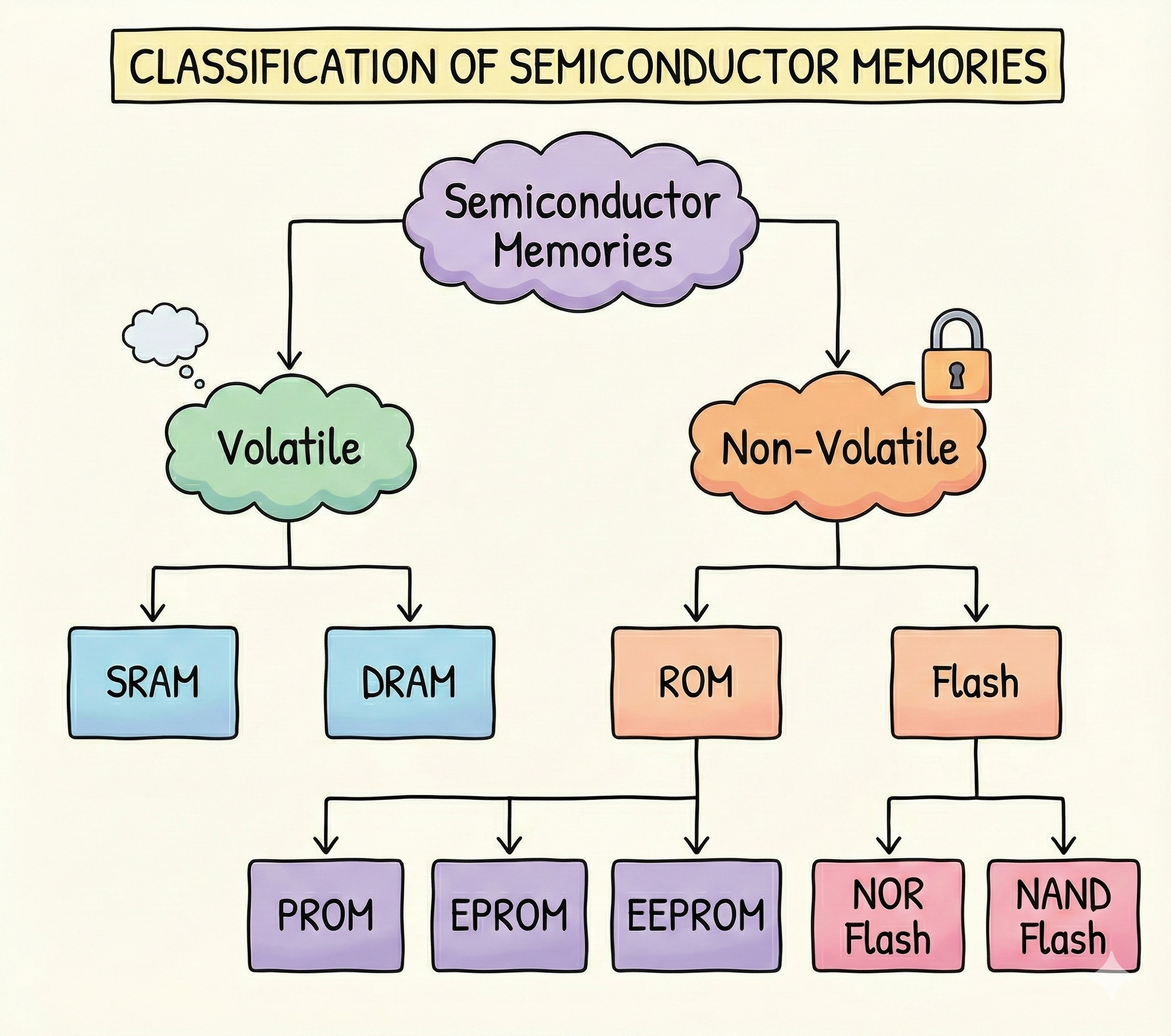
The semiconductor memory landscape is broadly categorized by volatility—the ability of a device to retain stored information when the power supply is removed.
The Memory Hierarchy
Volatile Memory: Loses stored data immediately when power is turned off. It is primarily used for temporary, high-speed tasks.
Non-Volatile Memory: Retains data even after the power is shut off. It is essential for long-term storage and firmware.
2. Volatile Memory (RAM)
Random-Access Memory (RAM) serves as the primary "working storage" in computing systems. It allows data to be read from and written to in any order, regardless of the physical location of the data inside the memory.
2.1 Dynamic RAM (DRAM)
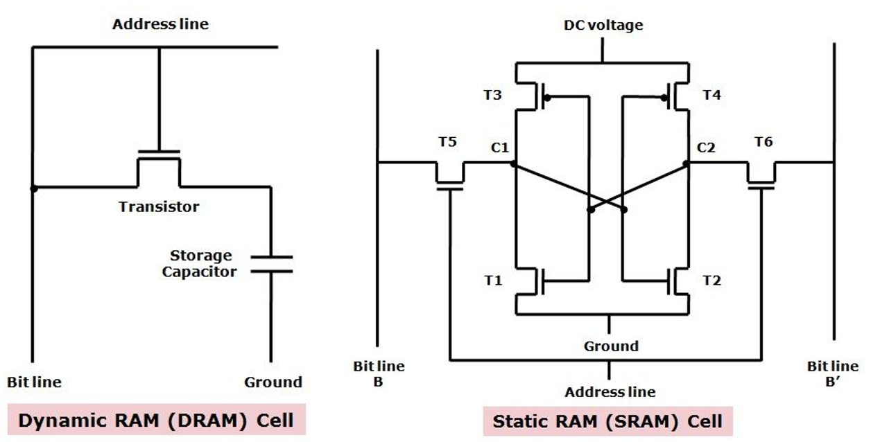
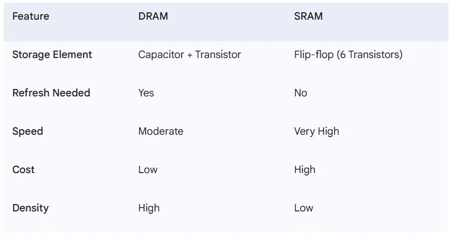
DRAM stores data as an electrical charge in a capacitor-transistor pair.
Operation: Because the charge in the capacitor leaks over time, it requires periodic refreshing to maintain data integrity.
Mechanism: When reading or writing, the address line is activated. The transistor acts as a switch: it is closed (allowing current to flow) if voltage is applied to the address line, and open (no current flow) if no voltage is applied.
Writing: A voltage signal is applied to the bit line—high voltage indicates logic 1, while low voltage indicates logic 0. The address line signal then enables the transfer of this charge to the capacitor.
Applications: It is the most cost-effective and common type used for main computer memory (PCs, game consoles, and graphics cards).
2.2 Static RAM (SRAM)
SRAM uses a flip-flop circuit to store data, typically requiring six transistors per cell.
Operation: Unlike DRAM, it does not require refreshing and is much faster, though more expensive and less dense.
Transistor Logic: To generate a stable logic state, four transistors (T1, T2, T3, T4) are organized in a cross-connected way.
Logic 1: Node C1 is high and C2 is low; in this state, T1 and T4 are off, while T2 and T3 are on.
Logic 0: Junction C1 is low and C2 is high; T1 and T4 are on, while T2 and T3 are off.
Access: Two additional transistors (T5 and T6) control the reading and writing processes via the address line.
Applications: Primarily used for high-speed applications like CPU cache.
3. Non-Volatile Memory
3.1 ROM, EPROM, and EEPROM
Read-Only Memory (ROM) traditionally contains the essential data required to boot a computer system. While early ROM was "hard-wired," modern versions have evolved:
EPROM (Erasable Programmable ROM): Can be erased using strong ultraviolet light.
EEPROM (Electrically Erasable Programmable ROM): Can be erased and reprogrammed electrically, paving the way for modern Flash memory.
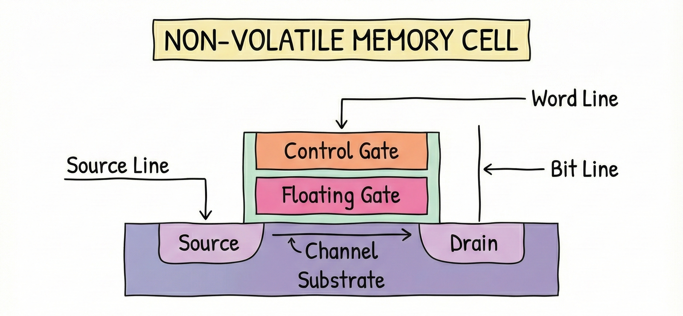
3.2 Flash Memory
Flash memory is a high-density type of EEPROM that allows data to be rewritten in large blocks rather than bytes. It is the backbone of USB drives, Solid State Drives (SSDs), and SD cards.
How Flash Cells Work
Flash memory cells use floating-gate transistors. The floating gate is electrically isolated by an oxide layer, allowing it to trap electrons.
Programming: A high voltage on the control gate causes electrons to tunnel through the oxide layer into the floating gate.
Retention: Because the gate is isolated, the charge remains even when power is removed.
Erasing: A large negative voltage forces electrons out of the floating gate, resetting the cell.
3.2.1 NAND vs. NOR Flash
NAND Flash: Offers high density and low cost. It is optimized for large-scale data storage (SSDs).
NOR Flash: Offers faster read speeds and random access, making it ideal for storing firmware and executable code.
3.2.2 NAND Density Levels (MLC)
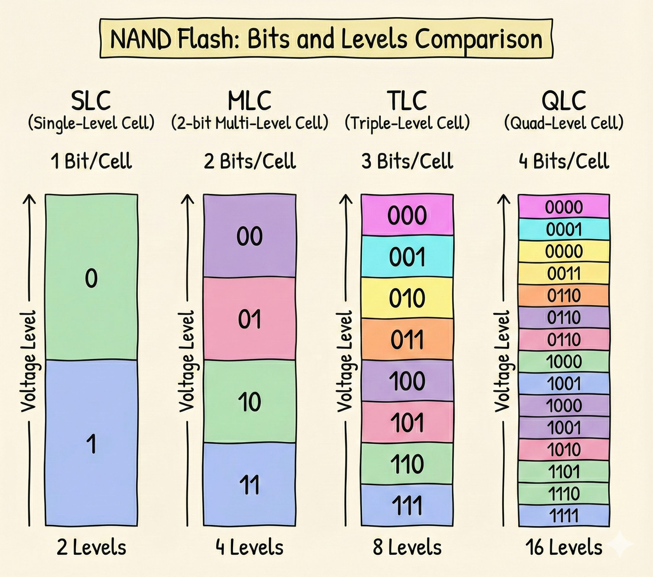
Engineers increase storage capacity by storing more bits per cell:
SLC (Single-Level Cell):2^1 = 2 levels.
MLC (2-bit Multi-Level Cell): 2^2 = 4 levels.
TLC (3-bit Multi-Level Cell): 2^3 = 8 levels.
QLC (4-bit Multi-Level Cell): 2^4 = 16 levels. A QLC cell can store the same amount of information in a chip size that is 67.5% smaller than an SLC cell.
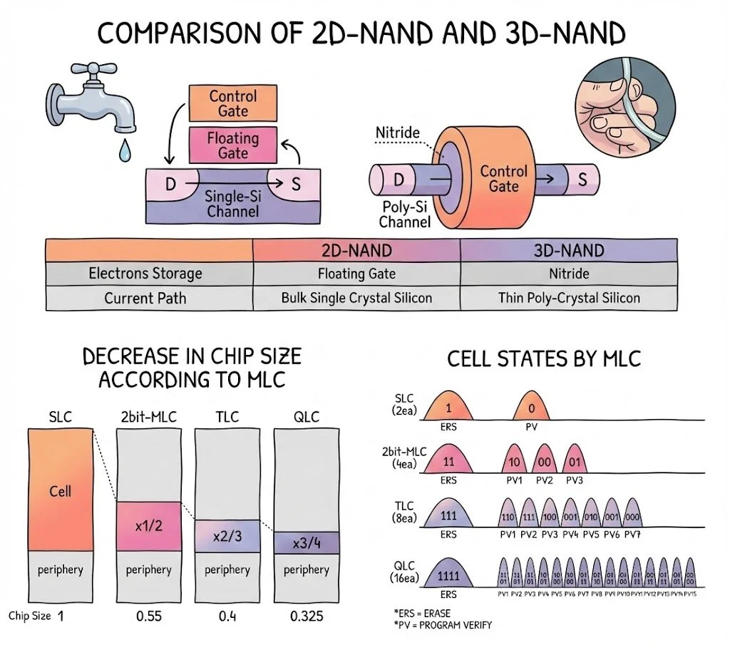
3.2.3 Architecture: From 2D to 3D and 4D NAND
NAND flash memory is currently undergoing a structural evolution from 2D (planar) to 3D and 4D architectures.
2D-NAND Scaling: Historically, capacity was increased through lateral scaling—shrinking the active gates to pack more cells into the same physical area. This was the primary industry focus until the early 2010s.
The Scaling Limit: Planar scaling eventually reached its physical threshold. Challenges such as the limitations of fine-patterning lithography and "lifespan issues"—where data integrity is lost over time due to cell-to-cell interference—made further lateral shrinking impossible.
3D-NAND Innovation: To overcome these barriers, manufacturers transitioned to 3D-NAND, which involves stacking memory cells vertically. This approach significantly increases density while improving reliability and longevity. Today, all major NAND manufacturers have shifted their development and production focus toward these vertical architectures.
4. Market Trends and Future Outlook
The NAND flash memory market was valued at USD 46.62 billion in 2020 and is expected to reach USD 85.36 billion by 2026, representing a CAGR of 11.27%.
Smartphones: NAND consumption is driven by the growth of average smartphone capacity. In 2017, the average phone had 43 GB of storage; by 2021, this grew to 142 GB, with flagship devices now reaching 1 TB.
Emerging Tech: Macro trends in AI, machine learning, and autonomous automotive systems are significantly increasing the demand for high-performance NAND packaging.

Key Industry Players
The landscape is dominated by leaders such as Samsung, SK Hynix, Micron, Western Digital.
5. References
NAND Flash Market Industry Analysis – GMInsights.
Semiconductor Memory – Wikipedia.
Electronics Engineering: Semiconductor Memory – GeeksforGeeks.