An inside view from the perspective of a CPU design engineer
When you look at a modern smartphone SoC, it is tempting to think of it as one enormous piece of silicon designed by one team.
It isn’t.
A modern SoC is the result of many engineering disciplines working together, each owning a different part of the journey from an architectural idea to a manufactured chip. As a CPU design engineer, I sit somewhere in the middle of that process: close enough to the architecture to understand what the CPU needs to do, but deep enough in the RTL to worry about how every piece of logic actually implements that behavior.
The die photograph below is a useful way to visualize the end result.
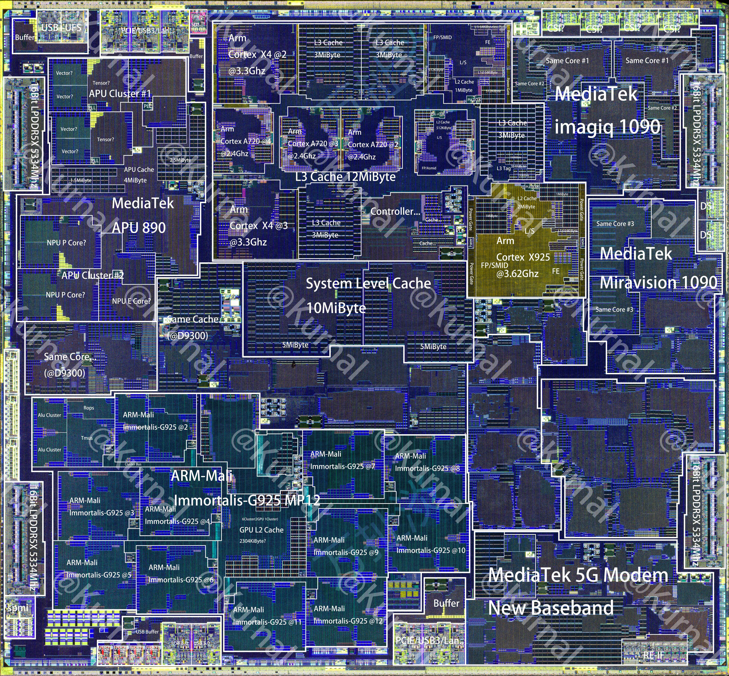
Image source: Kurnal Insights
The CPU is only one part of the SoC
It's beautiful yet confusing, isn't it ?
The image above contains many different blocks: CPU cores and caches, graphics, NPU/AI accelerators, multimedia, memory interfaces, display and camera logic, connectivity, modem/baseband, and a large amount of infrastructure that connects everything together.
The CPU complex is only one region of that much larger system.
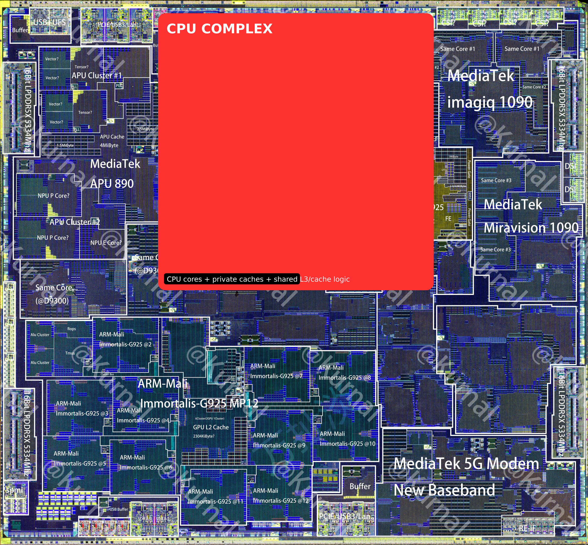
Image source: Kurnal Insights
The highlighted region is intended to give a visual sense of the CPU complex: the CPU cores, their cache hierarchy, and the surrounding logic required to make the CPUs operate as part of the SoC.
What is particularly interesting is that the block you see in the final die photo represents the work of many different teams.
From my perspective as a CPU design engineer, four groups are particularly important:
- System architects
- RTL design engineers
- Verification engineers
- Physical design engineers
They have different skill sets, different tools, and different definitions of success. But they are all working toward the same goal: turning a specification into working silicon.
1. System Architects — Deciding What to Build
Before anyone writes RTL, somebody has to decide what the CPU and the SoC should actually do.
That is the job of the system architecture team.
An architect works at a higher level of abstraction than an RTL designer. Rather than thinking primarily about individual registers, state machines, and clock cycles, architects think about the behavior and organization of the complete system.
The architect is effectively defining the contract that the implementation teams have to satisfy.
Architecture is about trade-offs
One of the interesting things about SoC architecture is that there is rarely a single “correct” answer.
Suppose we want more CPU performance.
We could:
- increase the number of cores,
- increase clock frequency,
- increase cache size
But every decision has consequences.
More cache consumes area.
Higher frequency increases timing pressure and often power.
More cores increase the coherency and interconnect complexity.
How do we manage thermals as a result of more performance?
The architecture team therefore has to optimize the whole system, rather than a single block.
The output of architecture
Eventually, the architectural ideas become much more concrete.
The architecture team produces specifications describing things such as:
- interfaces,
- protocols,
- performance requirements,
- memory maps,
- coherency behavior,
- exception behavior,
- power states,
- clocking requirements,
- security requirements,
- and functional requirements.
That specification becomes the starting point for the implementation and verification teams.
2. RTL Design Engineers — Turning Architecture Into Hardware
As an RTL design engineer, the job is to take the architectural specification and turn it into digital hardware.
RTL stands for Register Transfer Level.
At this level, we describe how data moves between registers and how combinational logic transforms that data.
For a CPU, this means implementing things such as:
- instruction fetch,
- instruction decode,
- register files,
- execution units,
- arithmetic and logical operations,
- load/store pipelines,
- branch handling,
- exception handling,
- control logic,
- cache interfaces,
- performance monitoring,
- debug interfaces,
- and many other pieces of the processor.
A CPU is not written as one giant block of RTL. It is broken into many smaller units, each with well-defined interfaces and responsibilities.
The most commonly used language in the industry is SystemVerilog, as it is natively supported across all major EDA toolchains.
From one generation to the next, it is rare for the whole design to be overhauled. Usually, we make incremental changes to specific parts of the design.
3. Verification Engineers — Trying to Break the Design
If RTL engineers build the hardware, verification engineers try very hard to prove that we built the right hardware.
This is one of the most important parts of CPU development.
A CPU can contain millions or billions of transistors, and the number of possible states and interactions is enormous. It is impossible to test every possible sequence manually. Once a design is taped out, that bug is permanent.
Verification therefore uses multiple techniques.
Two important ones are simulation-based verification using UVM and formal verification.
In big design houses, verification and design are usually separate specialized teams. Verification engineers build and maintain the testbench environments that we designers rely on to validate our changes.
A good verification engineer thinks like a skilled hacker: adept at pushing the design into obscure corner cases where bugs are most likely to hide.
3.1 Simulation-Based Verification (UVM)
UVM — the Universal Verification Methodology — is widely used for building reusable SystemVerilog verification environments.
Instead of simply applying a few hand-written tests to the CPU, a verification environment can generate large numbers of transactions and instruction sequences.
A simplified environment might look like:
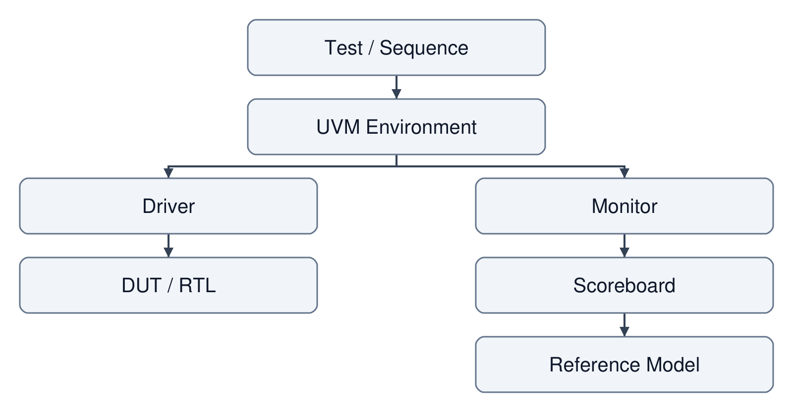
The verification environment can generate stimulus, observe the RTL, and compare the results against an expected behavior.
Functional simulation of RTL is performed using industry-standard logic simulators, most notably Synopsys VCS, Siemens QuestaSim, and Cadence Xcelium.
3.2 Formal Verification — Proving Properties
Simulation asks:
“Did the design behave correctly for all the tests we ran?”
Formal verification approaches the problem differently.
It can ask:
“Can I mathematically prove that this property always holds?”
For example, suppose a design contains an arbitration mechanism.
We might have a property such as:
    If request A is granted,
    then request B cannot also be granted
    at the same time.
Formal tools can explore the possible states of the design and attempt to prove that the property is always true.
This is particularly useful for control logic, protocols, arbiters, FIFOs, state machines, security properties, and many other pieces of hardware where exhaustive simulation would be impractical.
Formal verification and simulation complement each other.
Neither replaces the other.
4. Physical Design Engineers — Turning RTL Into Silicon
At this point we have something that behaves like a CPU in simulation.
But we still don’t have a physical chip.
RTL describes logical behavior.
A physical design engineer has to turn that logical description into an actual physical implementation consisting of transistors, standard cells, wires, clocks, power distribution, and physical structures.
This is where the design begins to look much more like the die photograph at the beginning of this article.
The physical design flow includes stages such as:
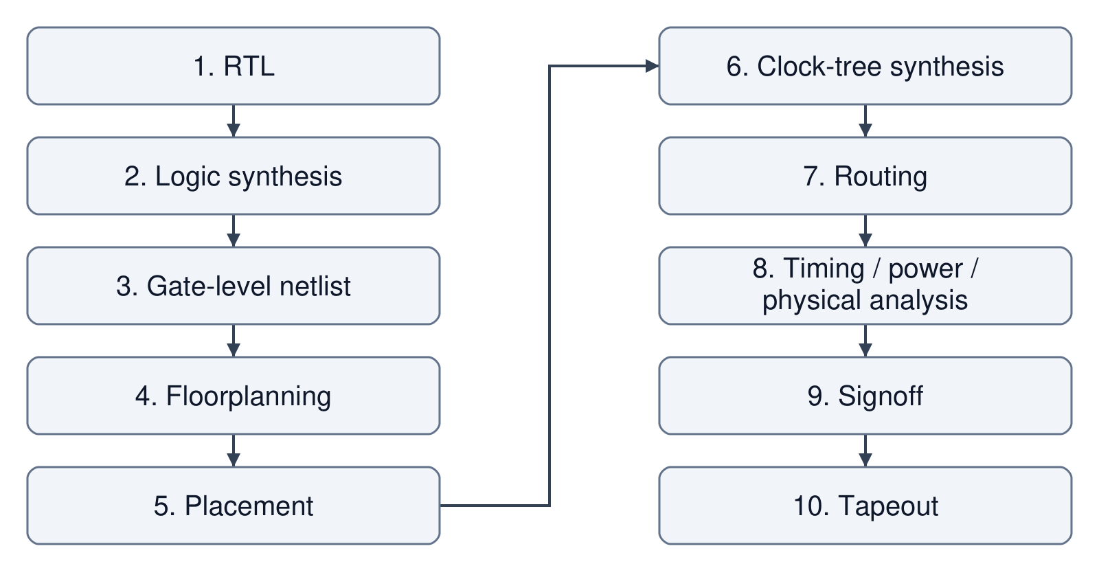
The exact flow is considerably more complicated than this simplified diagram, but the basic idea is that the logical design eventually becomes a physical layout.
Floorplanning
One of the first major physical questions is:
Where should all the blocks go?
This matters enormously.
Imagine placing two blocks that exchange huge amounts of data on opposite sides of the chip.
The logic may be functionally correct, but the long wires can create:
- timing problems,
- additional power consumption,
- routing congestion,
- signal-integrity problems,
- and area inefficiency.
So physical design is not simply “drawing the RTL onto silicon.”
The physical implementation feeds back into architectural and RTL decisions.
Timing — When Does the Signal Arrive?
One of the most important constraints in a CPU is timing.
Suppose one piece of logic produces a result that another piece of logic needs to consume on the next clock cycle.
The signal has to travel through:

The total delay must fit within the available clock period.
If the CPU is running at 3 GHz, one clock cycle is only about:
1 / 3 GHz ≈ 333 ps
That is an extremely small amount of time.
Every logic gate, multiplexer, wire, buffer, and physical effect matters.
This is why a CPU that is functionally correct in RTL simulation can still fail to meet its frequency target after physical implementation.
The RTL designer and physical design engineer therefore have a close relationship.
If timing is failing, the solution might involve:
- changing the RTL,
- adding or moving pipeline stages,
- restructuring logic,
- changing a microarchitectural decision,
- improving placement,
- changing buffering,
- or changing physical constraints.
Power, Performance, and Area (PPA)
Throughout the process, engineers are constantly balancing three fundamental constraints:
Power, Performance and Area — PPA.
For example:
| Decision | Possible benefit | Possible cost |
|---|---|---|
| Larger cache | Better performance | More area and power |
| More pipeline stages | Higher frequency | More complexity and potential penalties |
| More execution units | More throughput | More area and power |
| Larger structures | More parallelism | More leakage/dynamic power |
| Higher voltage/frequency | More performance | Higher power |
The architecture team makes high-level PPA decisions.
RTL designers optimize the implementation.
Verification engineers make sure those optimizations don’t break functionality.
Physical design engineers determine whether the implementation can actually be built and meet its physical targets.
The Real Flow: An Iterative Loop, Not a Conveyor Belt
It is tempting to imagine SoC development as a simple pipeline:
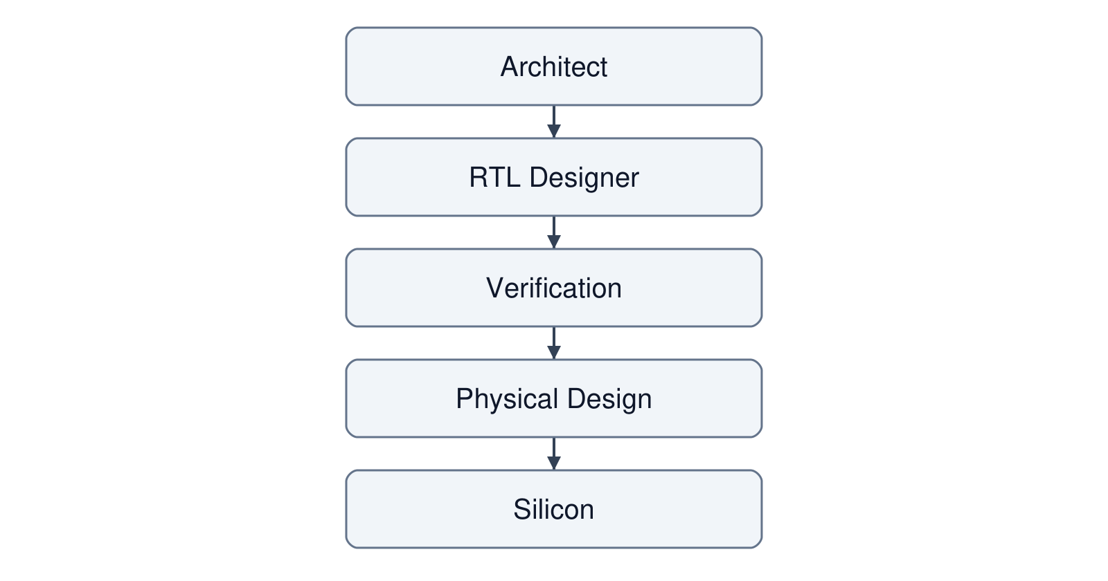
Real chip development is much more iterative.
A more realistic picture is:
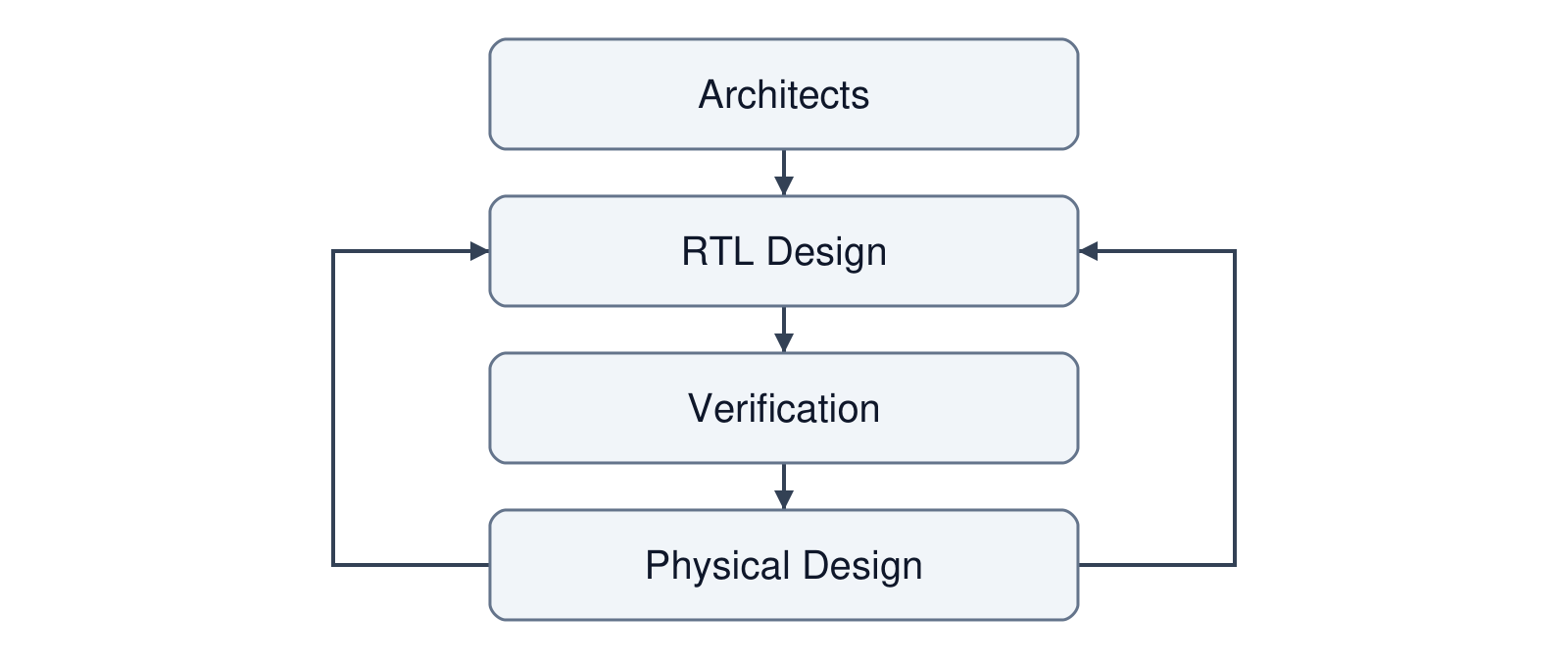
Verification finds a bug.
The RTL team fixes it.
Physical design discovers a timing problem.
The RTL team changes the implementation.
Power analysis reveals that a block is too expensive.
Architects reconsider the design trade-off.
A new architectural requirement appears.
Everyone goes back to work.
This iteration is one of the defining characteristics of modern SoC development.
From Tapeout to Working Silicon
Eventually, after architecture, RTL implementation, verification, physical design, and many rounds of iteration, the design reaches tapeout.
The fabless semiconductor company sends the final physical design to a semiconductor foundry.
The foundry manufactures the silicon.
After fabrication comes another set of engineering challenges:
- wafer testing,
- packaging,
- bring-up,
- validation,
- characterization,
- performance testing,
- power testing,
- and eventually production.
Only then does the CPU design that started as an architectural specification become the physical silicon that you can see in a die photograph.
And that is the part that is easy to forget when looking at an SoC like this.
Every rectangular region on the die represents an enormous amount of engineering work.
Behind a CPU cluster are architects deciding what it should be.
Behind the RTL are engineers turning that specification into hardware.
Behind the verification results are engineers trying to find the bugs before customers do.
Behind the physical layout are engineers making sure the design can actually operate at the required speed, power and area.
Useful Resources
Intel has published insightful behind-the-scenes videos detailing the Panther Lake development process, illustrating the broad range of teams and skill sets required to build a modern SoC: